Transistor is a semiconductor device capable of providing amplification of electric power and having three or more electrodes.
See also: diode symbols ►
| Symbol | Description |
|---|---|
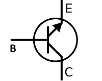
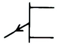
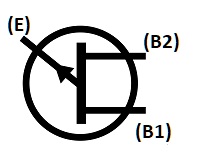
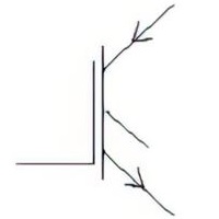
 | Name: PNP transistor Remark: Also PNIP transistor, if omitting the intrinsic region will not result in ambiguity. Source: IEC 60617-2019, ANSI/IEEE Std 315A-1986 |
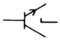
 | Name: PNP transistor Remark: Also PNIP transistor, if omitting the intrinsic region will not result in ambiguity. C – Collector, B – Base, E – Emitter. Source: IEEE Std 315-1993, ANSI/IEEE Std 315A-1986 |
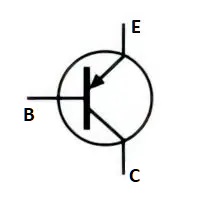
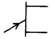
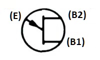
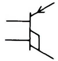
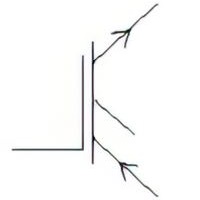
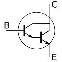
 | Name: NPN transistor Remark: Also NPIN transistor, if omitting the intrinsic region will not result in ambiguity. C – Collector, B – Base, E – Emitter. Source: IEC 60617-2019 |
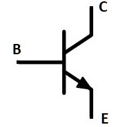
 | Name: NPN transistor Remark: Also NPIN transistor, if omitting the intrinsic region will not result in ambiguity. C – Collector, B – Base, E – Emitter. Source: IEEE Std 315-1993 |
 | Name: NPN transistor with collector connected to the envelope Source: IEC 60617-2019, ANSI/IEEE Std 315A-1986 |
 | Name: NPN avalanche transistor Source: IEC 60617-2019, ANSI/IEEE Std 315A-1986 |
 | Name: Unijunction transistor with P-type base Source: IEC 60617-2019, ANSI/IEEE Std 315A-1986 |
 | Name: Unijunction transistor with P-type base Remark: B – Base, E – Emitter Source: IEEE Std 315-1993, ANSI/IEEE Std 315A-1986 |
 | Name: Unijunction transistor with N-type base Source: IEC 60617-2019, ANSI/IEEE Std 315A-1986 |
 | Name: Unijunction transistor with N-type base Remark: B – Base, E – Emitter Source: IEEE Std 315-1993, ANSI/IEEE Std 315A-1986 |
 | Name: NPN transistor with transverse biased base Source: IEC 60617-2019, ANSI/IEEE Std 315A-1986 |
 | Name: NPN transistor with transverse biased base Remark: B – Base, E – Emitter, C – Collector Source: IEEE Std 315-1993, ANSI/IEEE Std 315A-1986 |
 | Name: PNIP transistor with connection to the intrinsic region Source: IEC 60617-2019, ANSI/IEEE Std 315A-1986 |
 | Name: PNIP transistor with ohmic connection to the intrinsic region Remark: B – Base, E – Emitter, C – Collector Source: IEEE Std 315-1993, ANSI/IEEE Std 315A-1986 |
 | Name: PNIN transistor with connection to the intrinsic region Source: IEC 60617-2019, ANSI/IEEE Std 315A-1986 |
 | Name: PNIN transistor with ohmic connection to the intrinsic region Remark: B – Base, E – Emitter, C – Collector Source: IEEE Std 315-1993, ANSI/IEEE Std 315A-1986 |
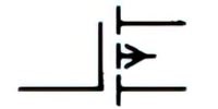
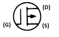
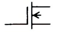
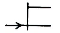 | Name: Junction field effect transistor with N-type channel Alternative name: JFET, N channel Remark: The gate and source connections shall be drawn in line. Source: IEC 60617-2019, ANSI/IEEE Std 315A-1986 |
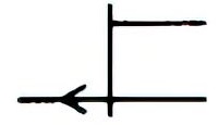
 | Name: Field-effect transistor with N channel Alternative name: JFET, N channel Remarks: If desired, the junction-gate symbol element may be drawn opposite the preferred source. G – Gate, D – Drain, S – Source Source: IEEE Std 315-1993, ANSI/IEEE Std 315A-1986 |
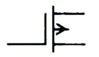
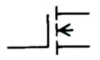
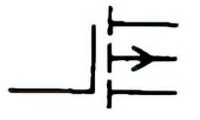
 | Name: Junction field effect transistor with P-type channel Alternative name: JFET, P channel Remark: The gate and source connections shall be drawn in line. Source: IEC 60617-2019, ANSI/IEEE Std 315A-1986 |
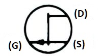 | Name: Field-effect transistor with P-channel (junction gate and insulated gate) Alternative name: JFET, P channel Remark: G – Gate, D – Drain, S – Source Source: IEEE Std 315-1993, ANSI/IEEE Std 315A-1986 |
 | Name: Insulated-gate bipolar transistor (IGBT) enhancement type, P channel Source: IEC 60617-2019 |
 | Name: Insulated-gate bipolar transistor (IGBT) enhancement type, N channel Source: IEC 60617-2019 |
 | Name: Insulated-gate bipolar transistor (IGBT) depletion type, P channel Source: IEC 60617-2019 |
 | Name: Insulated-gate bipolar transistor (IGBT) depletion type, N channel Source: IEC 60617-2019 |
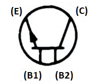
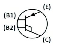
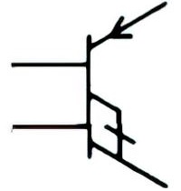
 | Name: Phototransistor Remark: PNP type is shown Source: IEC 60617-2019 |
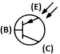 | Name: Phototransistor (PNP-type) Remark: B – Base, C – Collector, E – Emitter Source: IEEE Std 315-1993, ANSI/IEEE Std 315A-1986 |
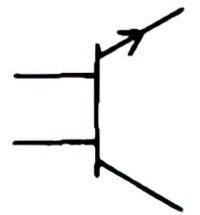
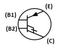
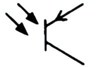
 | Name: Darlington transistor (NPN-type) Source: IEEE Std 315-1993 |
IGFET (MOSFET) Transistor Symbols
Notes:
- Insulated-gate field-effect transistor (IGFET) is a field-effect transistor having one or more gate electrodes which are electrically insulated from the channel.
- Metal-oxide-semiconductor field-effect transistor (MOSFET) is an insulated-gate field-effect transistor in which the insulating layer between each gate electrode and the channel is oxide material.
| Symbol | Description |
|---|---|
 | Name: Insulated gate field effect transistor IGFET enhancement type, single gate, P-type channel without substrate connection Remark: For an example with multiple gates, see symbol S00679. Source: IEC 60617-2019, ANSI/IEEE Std 315A-1986 |
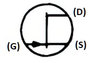
 | Name: Insulated gate field effect transistor IGFET, depletion type, single gate, P-type channel without substrate connection Source: IEC 60617-2019, ANSI/IEEE Std 315A-1986 |
 | Name: P-channel insulated-gate, depletion-type, single-gate, passive-bulk (substrate), three-terminal device Remark: G – Gate, D – Drain, S – Source Source: IEEE Std 315-1993, ANSI/IEEE Std 315A-1986 |
 | Name: Insulated gate field effect transistor IGFET enhancement type, single gate, N-type channel without substrate connection Source: IEC 60617-2019, ANSI/IEEE Std 315A-1986 |
 | Name: Insulated gate field effect transistor IGFET, depletion type, single gate, N-type channel without substrate connection Source: IEC 60617-2019, ANSI/IEEE Std 315A-1986 |
 | Name: N-channel insulated-gate, depletion-type, single-gate, passive-bulk (substrate), three-terminal device Remark: G – Gate, D – Drain, S – Source Source: IEEE Std 315-1993, ANSI/IEEE Std 315A-1986 |
 | Name: Insulated gate field effect transistor IGFET enhancement type, single gate, P-type channel with substrate connection brought out Source: IEC 60617-2019, ANSI/IEEE Std 315A-1986 |
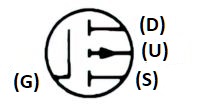 | Name: P-channel insulated-gate, enhancement-type, single-gate, active-bulk (substrate) externally terminated, four-terminal device Remark: G – Gate, D – Drain, U – Substrate (bulk), S – Source Source: IEEE Std 315-1993, ANSI/IEEE Std 315A-1986 |
 | Name: Insulated gate field effect transistor IGFET enhancement type, single gate, N-type channel with substrate internally connected to source Source: IEC 60617-2019, ANSI/IEEE Std 315A-1986 |
 | Name: N-channel insulated-gate, depletion-type, single-gate, active-bulk (substrate) internally terminated to source, three-terminal device Remark: G – Gate, D – Drain, S – Source Source: IEEE Std 315-1993, ANSI/IEEE Std 315A-1986 |
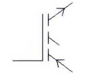
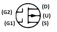
 | Name: Insulated gate field effect transistor IGFET, depletion type, two gates, P-type channel with substrate connection brought out Remark: In the case of multiple gates, the primary gate and the source connection shall be drawn in line. Source: IEC 60617-2019, ANSI/IEEE Std 315A-1986 |
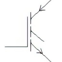
 | Name: P-channel insulated-gate, depletion-type, two-gate, five-terminal device Source: IEEE Std 315-1993 |